Electron-induced Secondary Electron Emission
Advanced Diagnostics Navigation
- Atomic and molecular species, positive and negative ions
- Laser-Induced Fluorescence (LIF) and Two-Photon Absorption LIF (TALIF)
- Radar Resonant Enhanced Multi-Photon Ionization (Radar REMPI)
- Characterization of plasma, chemical composition and dynamic behavior
- Electron velocity distribution function, gas flow velocity and temperature
- Electric field and space potential
- Nanoparticle Diagnostics
- Surface Diagnostics
Electron-induced Secondary Electron Emission and Surface Charging Measurements
Measurement of total secondary electron emission yield
Can measure both conducting and dielectric samples
Surface charging measurement with accuracy for the surface potential of 2 mV and spatial resolution of 1 mm
Primary electron beam energy 10 < Eb < 1000 eV
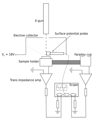
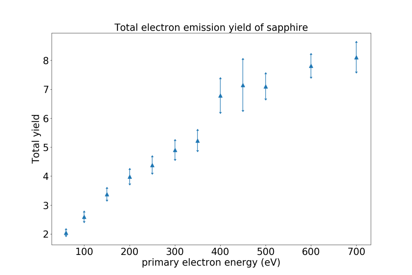
When a material gets irradiated by charged particles, the material may emit so-called secondary electrons. The amount of emitted secondary electrons depends on the beam energy and the angle of the primary beam to the substrate surface and can be different for different materials. Our setup (Fig. 1) is dedicated to measurements of electron-induced secondary electron emission (SEE). The SEE yield is ratio between the emitted secondary electrons and the incident electrons. Our setup can measure the total SEE yield where it does not distinguish between secondary or back scattered electrons. For non-conductive materials, a short, single pulse operation allows to minimize surface charge build-up. We usually limit the pulse duration to 6 microseconds. Moreover, recent additions to the experimental setup- a contactless surface potential probe – allows one to also measure the surface potential as well as the surface charge distribution built up due to the irradiation of the sample under investigation by electron beam. These measurements can be done without disturbing the state of the sample. An example of the SEE yield as the function of the energy of primary electrons (beam electrons) bombarding a sapphire sample is shown in Fig. 2.
Plasma parameters such as electron energy distribution, plasma density and the ionization dynamics are affected by SEE. Hence, it is of great importance to fully understand the SEE characteristics of a given plasma facing material, especially when considering dielectrics.
- A. Dunavesky, Y. Raitses and N. J. Fisch, “Yield of Secondary Electron Emission from Ceramic Materials of Hall Thruster”, Phys. Plasmas 10, 2574 (2003)
- Yevgeny Raitses, Paul Dourbal and Rostislav Spektor, “Secondary Electron Emission Properties of Boron Nitride Ceramic Materials at High Temperatures” IEPC-2015-342 /ISTS-2015-b-342, Joint Conference of 30th International Symposium on Space Technology and Science 34th International Electric Propulsion Conference and 6th Nano-satellite Symposium, Hyogo-Kobe, Japan July 4-10, 2015
- A.M. Capece, M.I. Patino, Y. Raitses and B. E. Koel, “Secondary electron emission from lithium and lithium compounds”, Appl. Phys. Lett. 109, 0011605 (2016)
- M. Patino, Y. Raitses and R. Wirz, “Secondary electron emission from a plasma-generated nanostructure tungsten fuzz”, Appl. Phys. Lett. 109, 201602 (2016)
- C. Jin, A. Ottaviano and Y. Raitses, “Secondary electron emission yield from high aspect ratio surfaces”, J. Appl. Physics 122, 173301 (2017)